Friday, December 11, 2015

Project on laser security system

LASER SECURITY SYSTEM

INTRODUCTION:
Laser security system is becoming popular system in stores, building and they are also becoming popular with private homes as well.the reason for becoming popular is due to its simplicity and efficient security.Basically it uses the IC 555 timer which has ability to produce long time delays in array of applications,has draw many designers from op-amp, mechanical timers and many discrete circuit into every increasing noxious timer users.So using IC 555 for laser security system which is also called as theft alarming system is the better choice.Basically in this system laser is focused on the  LRD mounted on board.However this is arrange there where the security is needed.Laser is focused on the LRD,so that if any theft try to gross the laser an if any blockage is recognize than alarm gets triggered.
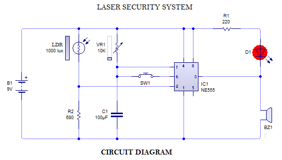


COMPONENTS REQUIRED:

  1. 9V battery with snap.
  2. Connecting wires.
  3. LDR(Light dependent Resistor).
  4. Variable resistance 10K ohms.
  5. Resistance 220 ohms, 680 ohms.
  6. LED.
  7. IC 555.
  8. Switch.
  9. Capacitor of 100 micro farad.
  10. Laser.
  11. Buzzer.

PCB LAYOUT:
This is how the layout looks when u have done with the designing.


WORKING:

  • This circuit uses IC 555,it basically connected as comparater with pin 6 with positive supply,whos output goes high then trigger pin 2 which is at supply lower than that of supply power,conversely the output goes low when it is 1/3.So the small change in voltage at pin 2 is sufficient to change the output of pin 3 from 1-0 or from 0-1.however output has 2 state ie. high and low which cannot remain in inbetween stage.It requires 9V of supply which can be provide with the battery itself,so it can be portable,hence the circuit is economical in power consumption.
  • To encounter the presence of theft we have LDR and a Laser.
  • LDR is an acronym for light dependent resistance.So as the name suggest it value is truly dependent on the intensity  of light,which is focused on he LDR. So it has resistance of 1 mega ohms in dark and 2-4 k ohms in day.Hence it is able to respond to a wide light spectrum.
  • Laser is focused on the LRD,so that if any theft try to gross the laser an if any blockage is recognize than alarm gets triggered.
You can watch the video below to know how the circuit works:


Thursday, December 10, 2015

convert live wire circuit diag to pcb layout using pcb wizard

Many student are usually afraid of designing PCB on its own it may be either due to working issue of designed PCB or they are unaware of how its done so what ever be the problem after reading this post u will be confident of at least trying it for once you just need to have a correct circuit diagram.Guys it is very easy than u think.The most important in PCB designing is  to convert the circuit diagram into layout.So the easiest software to do so is the PCB wizard.However PCB wizard  usually come with the live wire but some time it has to download and install separately.also keep in mind that live wire and PCB are the two different software,PCB wizard usually use in converting the live wire circuit into layout so it is a separately designing software which work in sink with the live wire.It is the most easiest way to convert the circuit diagram into layout,so the procedure to do is very simple.Now lets move to the procedure that need to be followed to convert using live wire and PCB wizard.
First u need to have pre-installed live wire and PCB wizard on your PC,If not installed then first install and after installing run the live wire software first,then draw the circuit on the live wire.After that check whether your circuit is working properly or not by clicking on the run button which present on the task bar of software or just press the F9 button it is the short cut command of live wire software.If circuit is working as per you plan,then go to the tool bar and in that u will be seeing the option such as simulation and design.Now click on the design but before moving to design make sure that you have opened PCB wizard on your PC then u can move to the design as explain above.after clicking on the design you will see a window click OK on that window after doing that it takes some time to design and automatically window will be displayed on which your circuit layout will be present.Hence that what you needed.
You can watch the video to know how its done.

To know more about live wire software u can read my post on PCB designing software u will get the details of the software and also the link for downloading the live wire and PCB wizard software in the same post and also there are many other post which will help u to develop you designing skills.Do check them out.

Monday, November 30, 2015

PCB Designing

A PCB has a copper track on the conducting sheet on which you can print the circuit layout and etch the PCB in the ferric chloride solution to design our circuit on the PCB this ensure that there is no wiring faults or the lose connection as our whole circuit is on the track only the thing we have to do is just solder the required components and provide the power supply to it to work.
Material required for designing will be:

  1. PCB.
  2. Laser printed layout of your circuit on the transparent sheet.
  3. white paper sheet or the thin cotton cloth
  4. Electric iron.
  5. Steel wool or scrotch bite.
  6. Plastic container.
  7. Etching solution.(Ferric chloride ie.FeCl3).
  8. Drill machine.
  9. Soldering iron.
Step 1: Take your PCB (it can be multi layered,double  layered or single layered).then remove the oxide and photo resist layer from the surface of the copper by scrubbing the top with the scrotch bite or steel wool care fully.
Step 2:Place your laser printed layout of your circuit on the PCB and upon that place white sheet or cotton cloth so that your transparent sheet do not stick the electric iron.
Step 3:Plug on the electric iron and let it be warm for some time,then start ironing the PCB till 5 min with pressure.
Step 4:Check whether the circuit has been printed on the board or not.If printed then stop the ironing and remove the sheet properly and slowly if you find that some of the circuit is not printed properly then do not remove it you continue your ironing till your circuit is properly printed.
Step 5:After your circuit properly imprinted on PCB ,then you can make the etching solution and dip your printed board in the solution and stir the solution slowly for 30 min then check that excess copper layer is removed or not.
Step 6:When done with etching you can now scrub you board to check the imprint of you circuit on the board.
Step 7:Start drilling hole using drilling machine on the PCB.
Step 8:Place your component at right place and bend the legs of component from behind so component doesn't fall off the board.
Step 9:start soldering the components.

Saturday, November 28, 2015

PCB circuit designing software


Mostly for designing the circuit and testing it  we require hardware as well as software .Basically hardware implementation of a circuit diagram may leads to the aging of component and components may also get damage if some thing went wrong while implementation.But considering the software implementation is quit easy and also cost effective as some software are made available for free on the webs to use, so if the testing is done first by using software will provide us knowledge of our circuit functioning and working as well while it also help us to prepare layout of the same without any error.With the software,circuit designing becomes easy and cost effective,so here is the software which would be very helpful for the second year engineering students.

Software:
live wire
This software is the most useful for the first year engineering student as it is easy to install as well as easy to operate this software as it gallery contains various categories such as power supply,connectors,active components,passive components,discrete semiconductors,logic gates,ICs,output comps and measuring.It provide easy designing and simulation with live to pay,pause or stop animation also provides user to check the running components as well as graphical outputs.In case you want to download the software you can download from below.
Click on the link to download the live wire:
This is the window which will appear every time when you open the software.

watch video to know more about live wire software:

Thank u for reading this post.
Hope this post have help u to understand the software,while there are another software also which is used to design circuit diagram such as proteus,eagle,etc but among them this is the easiest one to use and understand.


PCB etching process

Electronic devices used nowadays uses the PCB for interconnection of various components use in device so that the size of the device reduces and there is no complexity for the user as well as the engineer.While the engineers are the ones who design n implements the circuit using PCB so today I'm posting this so that the student who are unable to etch will be able to etch the PCB correctly without any hurdle.Following are the steps involve in PCB Etching:

Step 1:First thing to be done is polish the PCB using scrotch bite or sand paper so that the impurity gets removed from the surface and the surface looks shinning.

Step 2:Place the circuit design properly on the the polished PCB.
note:Your circuits laser print should be on on the transparent sheet so that the design will get imprinted on the PCB.

Step 3:Ironing
before start to iron your sheet should be covered with some cloths so that the sheet doesn't melt.

Step 4:After ironing for 5 min check that your circuit has been printed on the PCB or not,if not then iron for some more time.

Step 5:After circiut is printed then make the solution of ferric chloride(etching) in some container and dip  the pcb in the solution.

Step 6:shake the solution containing container till your PCB is been etched fully.
 Last not the least please dispose the solution properly.